Manoes, a reader of this blog, have send to me a description of a set of modifications for the « D6 » analyzer (My words remains in italics).
Mod’s I made.
I did put a lot of C’s 100pf on existing and newly made places on the powerline traces.
I also did try one on the input C it did not have effect that I expected but…… my measurement could be false, maybe someone can do it again.
Upside
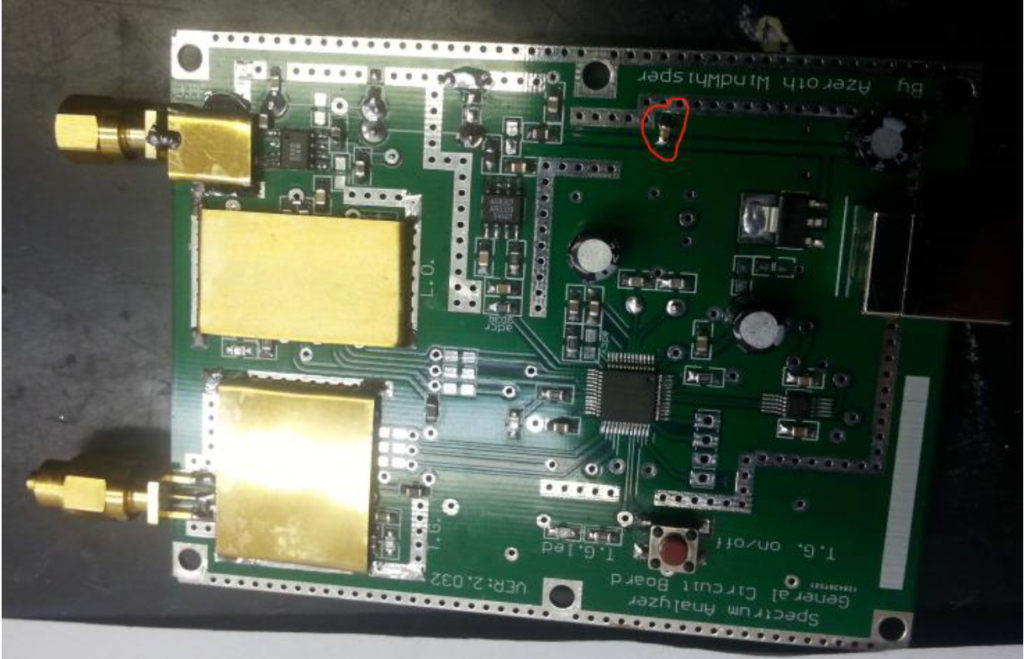
Upside of the board; maybe I forgot some C’s to mention but better one to much then one forgotten
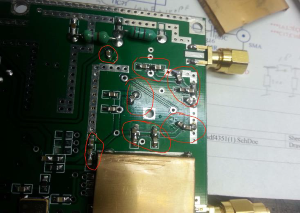
Underside of the board a lot of them, the places are experimental found…..
Just try and error with a non-conductive plier!!
Also I made some new screening on the upside and underside of the board.
I did change the SMA connectors for a wider type witch has nuts on the outside.
Before I put the whole board inside the cabinet I glued some conductive foam on the board it did give a bit better result.
All the measurements are made with input and output closed with 50 Ohm the last picture is input and output connected with a short SMA cable.
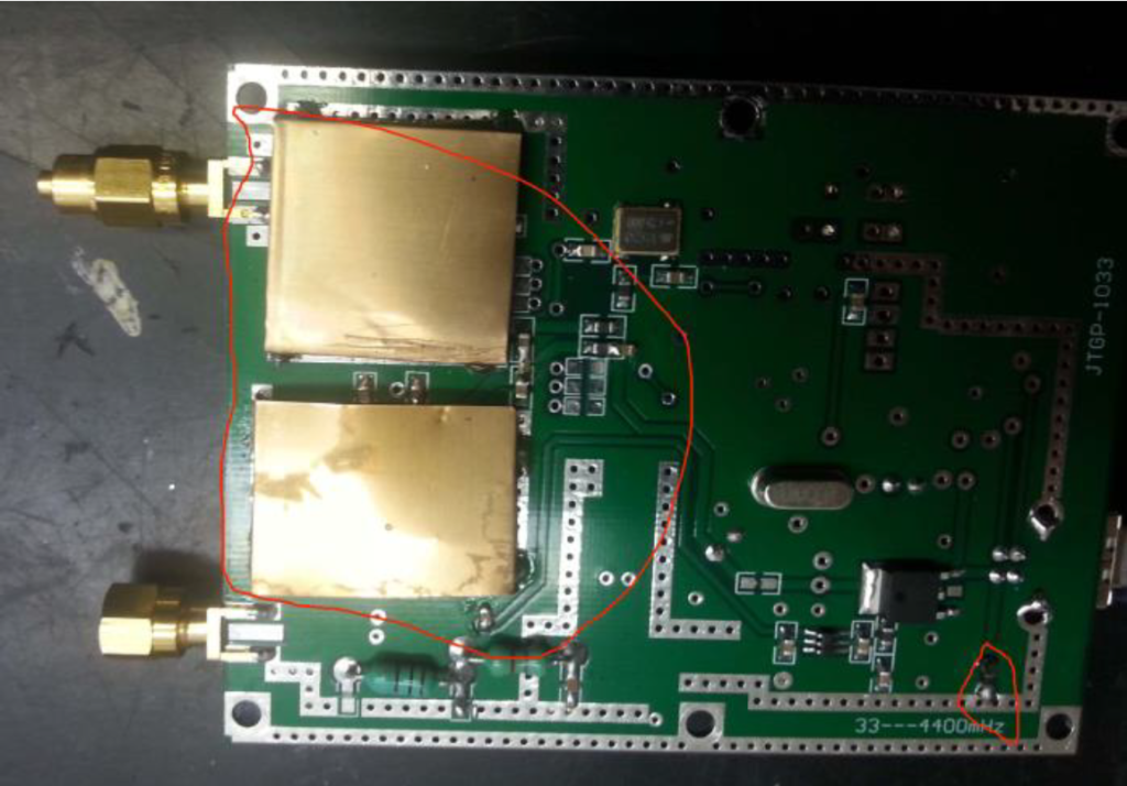
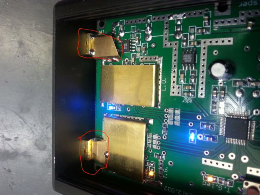
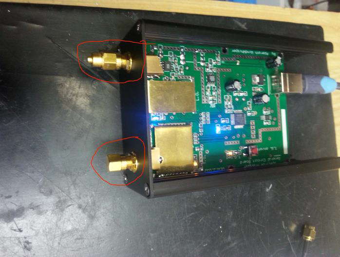
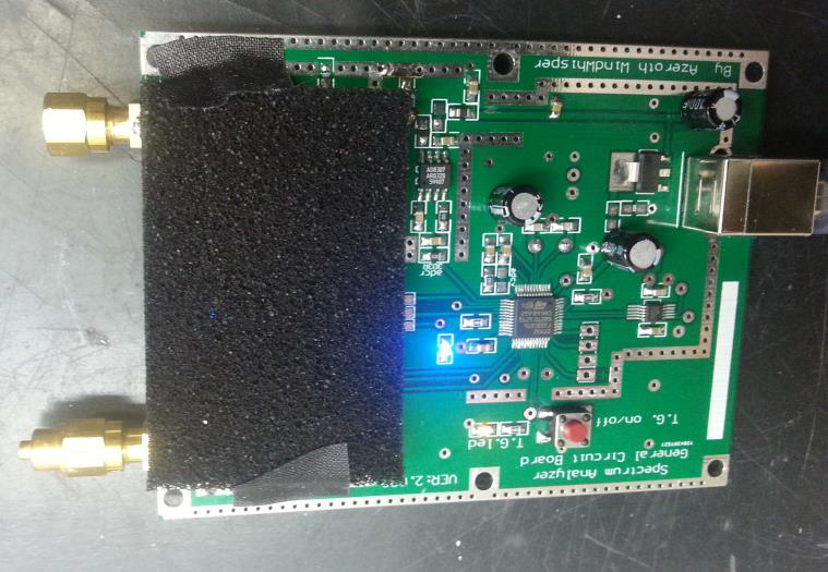
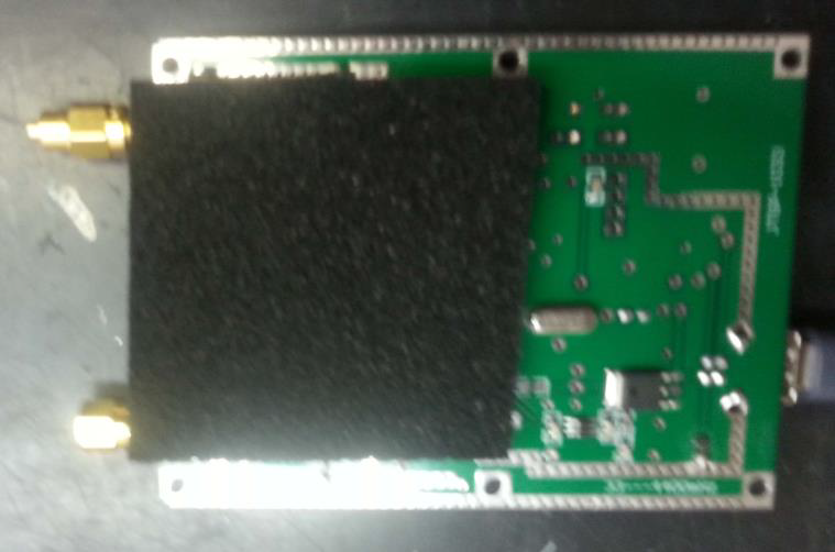
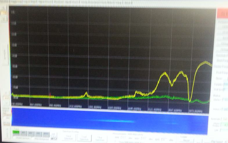
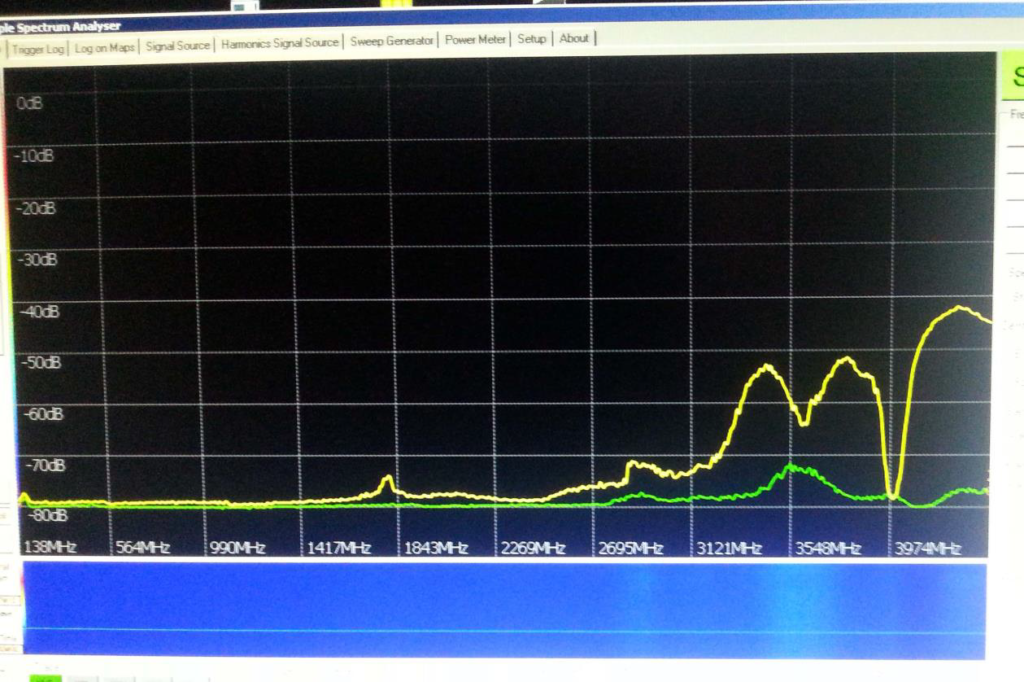
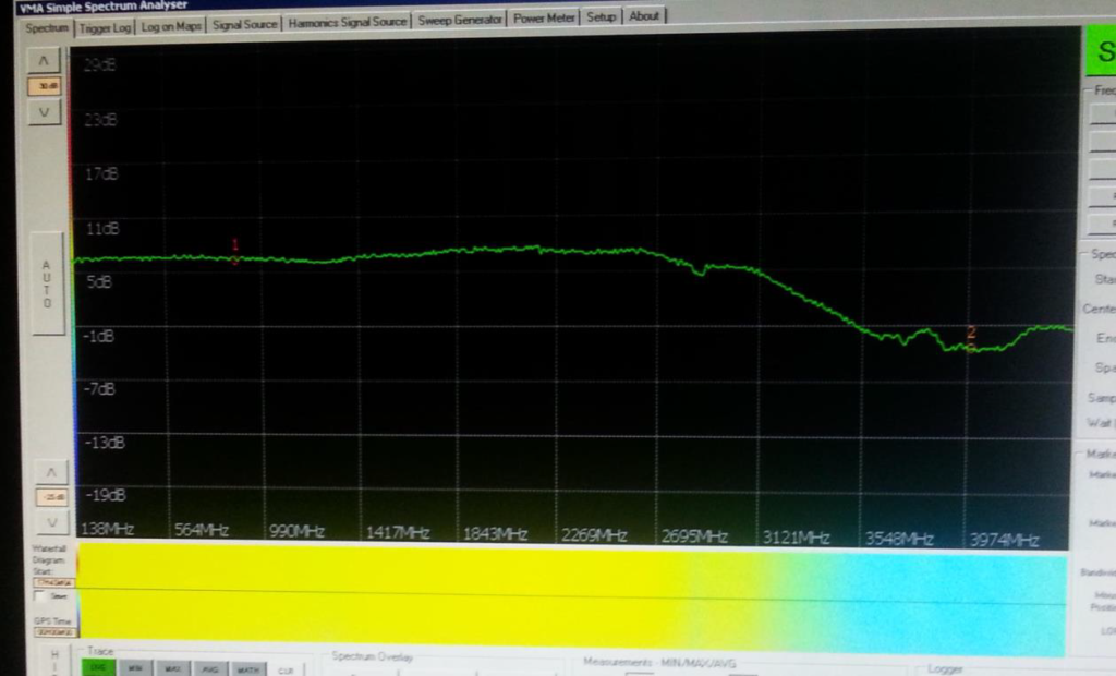
All the measurements are made with the above mods. Terrible enough my spectrumanalyser is broken during the measurements so I can not produce better pictures as above ones. I do hope to repair the old boy when I have the time to live and fun to do it. (High tension unit defect, transformer into smoke so I have to made a new one by hand .
Software VMA of our friend Vitor Martins Augusto.
Grtz, Manoes
For several months i don’t understand why the frequency response curve of this analyzer deteriorated when we exceeded 3GHz. By drastically reducing this problem Manoes give me an answer.
I will add an option on SNASharp to be able to trace the frequency response of an analyzer by disabling the calibration, this can help to understand how a hardware modification work.
David.
